#Industry (Production, process)
Toshiba Proposes Superlattice Underneath Transfer Gate
The dark current and white pixel defects are also said to be reduced
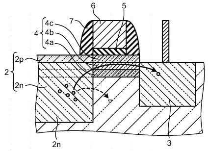
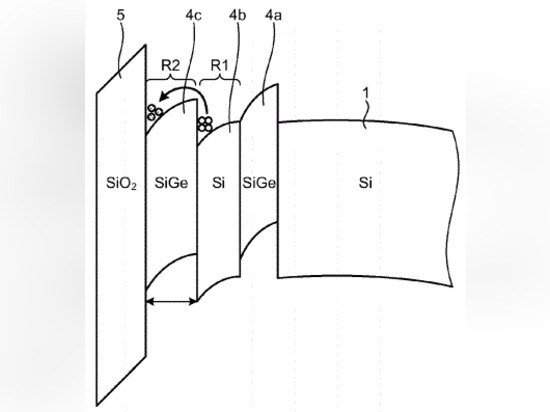
Toshiba patent application US20150008482 "Semiconductor device and manufacturing method thereof" by Motoyuki Sato says that making SiGe superlattice under transfer gate can drastically reduce the influence of SiO2/Si interface traps that potentially can capture photoelectrons during the transfer.

